Для моей лекции по встроенным системам мне нужно беспроводное соединение с роботом, которого мы будем разрабатывать в течение этого курса. Пока у меня SMAC (IEEE802.15.4) и Bluetooth отработаны. Но этот IEEE802.15.4 (ZigBee) стоит дорого, а дешевые модули Bluetooth отлично подходят для соединения между роботом и хостом, но не для роботов, которые должны взаимодействовать друг с другом. Алекс Веккио (см. Этот пост ) указал мне на беспроводной модуль стоимостью $ 2,75 (!) С Nordic Semiconductor nRF24LU1 + . Именно то, что мне было нужно, с невероятно низкой ценой  .
.

nRF24L01 + Информация о модуле
Поэтому я заказал несколько модулей, и через несколько часов у меня было два FRDM-KL25Z, разговаривающих друг с другом:

Настройка nRF24L01 + с FRDM-KL25Z
Итак, вот что я задокументировал при разработке моего первого приложения с двумя модулями FRDM-KL25Z и двумя модулями nRF24L01 + …….
Nordic Semiconductor nRF24L01 +
Nordic Semiconductor оснащена беспроводным решением nRF24L01 + со сверхнизким энергопотреблением 2,4 ГГц в диапазоне ISM.
Обратите внимание, что версия «+» является более новой и рекомендуется к использованию. Имейте в виду, что некоторые поставщики модулей все еще могут продавать не + версию.
Ключевые характеристики nRF24L01 +: (источник: технические характеристики nRF24L01 + ):
- Во всем мире 2. ГГц ISM-диапазон (свободная нелицензионная полоса)
- Скорость передачи данных 250 кбит / с, 1 Мбит / с и 2 Мбит / с
- Сверхнизкое энергопотребление (11,3 мА Tx при выходной мощности 1 мВт, до 26 мкА в режиме ожидания I и 900 нА в режиме отключения питания)
- Напряжение питания 1,9 — 3,6 В, с допустимыми входными контактами 5 В
- Автоматическое подтверждение отправки с автоматическим повтором
- RX и TX FIFO с возможностью получения пользовательских данных ACK
- До 6 каналов данных / адресов для упрощенной звездной сети
- Простой 8-контактный (7-контактный без IRQ) интерфейс SPI: VCC, GND, CE, CSN, SCK, MISO, MOSI и дополнительный IRQ.
Я заказал мой на yourduino.com, который продает модуль всего за $ 2,75, см. Здесь макет и схемы ):

Модуль nRF24L01 +
 Если вы ищете в Интернете, многие другие поставщики продают этот модуль тоже, менее чем за 5 долларов.
Расположение модуля:

Макет NRF24L01 и контакты (Источник: GitHub )
Схема модуля:

Схема nRF24L01 (Источник: GitHub )
Блок-схема nRF24L01 +:

nRF24L01 Block Diagram (Source: Nordic Semiconductor Data Sheet nRF24L01P_Product_Specification_1_0.pdf)
Pin and SPI Connection
The module has following pins connecting to a microcontroller:
- GND: Ground.
- VCC: 3.3V.
- CE: Chip (RX/TX) Enable, high active. If high, module is either sending or listening.
- CSN: Chip Select Not, low active. If low, the chip responds to SPI commands. This is actually the ‘real’ chip select signal, and is easily confusing with CE which enables/disables the transceiver radio part.
- SCK: SPI Shift Clock, up to 10 MHz.
- MOSI: Master-Out-Slave-In, used to shift data from the microcontroller to the device.
- MISO: Master-In-Slave-Out, used to shift data from the device to the microcontroller.
- IRQ: Optional Interrupt Request pin. Signals RX/TX status like packet sent or received.
Bit/Byte order: The SPI needs to be configured to send the Most Significant Bit First. within a byte. For multiple data bytes, the Least Significant Byte needs to be shifted first.
Sender and Receiver Application
Time to get some hands-on! For this I’m using two RF modules with two FRDM-KL25Z. One board is sending data to the other, and they indicate with LED blinking proper operation. I’m using interrupts, but to keep things simple, I will only set a flag in the ISR I will do the radio processing outside of the interrupt service routine.
 Just setting a flag in the ISR keeps the interrupt service routine short and sweet, and I do not block further interrupts by accessing the radio module over the SPI bus. Additionally I use the SPI bus with interrupts, so doing interrupt-based SPI within another interrupt needs careful interrupt level planning. To keep things simple, I will not do this here.
Hardware Wiring
First, I need to wire the RF module to the processor. I’m using Processor Expert with CodeWarrior as this simplifies a lot. In this tutorial I’m using the following pin mapping:
=================================================================
 SIGNAL LIST
-----------------------------------------------------------------
SIGNAL-NAME [DIR]        => PIN-NAME [PIN-NUMBER]
-----------------------------------------------------------------
LED_BLUE [Output]        => ADC0_SE5b/PTD1/SPI0_SCK/TPM0_CH1 [74]
LED_GREEN [Output]       => TSI0_CH12/PTB19/TPM2_CH1 [54]
LED_RED [Output]         => TSI0_CH11/PTB18/TPM2_CH0 [53]
RF_CE [Output]           => PTB9 [48]
RF_CSN [Output]          => PTB8/EXTRG_IN [47]
RF_IRQ [Input]           => PTD0/SPI0_PCS0/TPM0_CH0 [73]
RF_MISO [Input]          => PTE3/SPI1_MISO/SPI1_MOSI [4]
RF_MOSI [Output]         => ADC0_SE7b/PTD6/LLWU_P15/SPI1_MOSI/UART0_RX/SPI1_MISO [79]
RF_SCK [Output]          => PTE2/SPI1_SCK [3]
=================================================================
- Make sure you have any extra components loaded (e.g. Wait and LED, see here).
- Create a Processor Expert project with the wizard (File > New Bareboard Project), then select your CPU and enable Processor Expert.
- Add the Wait component to your project. It is optional, and I’m using it in the demo application to wait for a given number of milli-seconds. Alternatively you can burn cycles in a loop.
- Add LED components to your project as needed (see this post). I’m using them to indicate the TX and RX status. Alternatively you can use BitIO component instead, or left it out.
- Now I’m going to add the components for the hardware connection to the module. If you are going to use different pins, then assign different pin names (of course).
- Add a BitIO component for CE: It is configured as output pin with initial LOW value. LOW means ‘not sending/listening’, so this is a good initialization value.
CE Properties
- Add a BitIO component for CSN: It is configured as output pin with initial HIGH value. CSN is pulled LOW to send commands to the transceiver.
CSN Properties
- Add an ExtInt component for the interrupt pin: The interrupt is active low, so we need to react on falling edge:
IRQ Properties
- Next to add SynchroMaster component for SPI:I need to assign the MISO, MOSI and CLK pins. Clock edge is on falling edge with MSB first, with LOW idle clock state. I’m using a fairly slow clock speed for now (it could go up to 10 MHz, but better to start slowly )
SPI Properties


For me it looks now like this:

Project with components
Source Files
With File > New > Source File and File New > Header File I’m adding
- Application.c: this is the application main file
- Application.h as interface for Application.c
- nRF24L01.c: Driver for the Transceiver
- nRF24L01.h interface to nRF24L01.c
The content of the files are posted at the end of this article. I’m explaining now what needs to be done to send and receive data. What is common is the initialization code.
Initialization
First, the application initilizes the driver and calls RF_Init():
WAIT1_Waitms(100); /* give device time to power up */
RF_Init(); /* set CE and CSN to initialization value */
Actually, it only sets the CE and CSN pins:
/*!
 * \brief Initializes the transceiver.
 */
void RF_Init(void) {
  RF_CE_LOW();   /* CE high: do not send or receive data */
  RF_CSN_HIGH(); /* CSN low: not sending commands to the device */
}
Next, it writes to configures the device using RF_WriteRegister(), configuring the output power (RF24_RF_SETUP_RF_PWR_0) and configures the data rate (250 kbit, RF24_RF_SETUP_RF_DR_250):
RF_WriteRegister(RF24_RF_SETUP, RF24_RF_SETUP_RF_PWR_0|RF24_RF_SETUP_RF_DR_250);
It is using the RF_SETUP (address 0×06) register:
| Address (Hex) | Mnemonic | Bit | Reset Value | Type | Description |
|---|---|---|---|---|---|
|
06
|
RF_SETUP
|
RF Setup Register | |||
|
CONT_WAVE
|
7
|
0
|
R/W | Enables continuous carrier transmit when high. | |
|
Reserved
|
6
|
0
|
R/W | Only ’0′ allowed | |
|
RF_DR_LOW
|
5
|
0
|
R/W | Set RF Data Rate to 250kbps. See RF_DR_HIGHfor encoding. | |
|
PLL_LOCK
|
4
|
0
|
R/W | Force PLL lock signal. Only used in test | |
| RF_DR_HIGH | 3 |
1
|
R/W | Select between the high speed data rates. This bitis don’t care if RF_DR_LOW is set.Encoding:[RF_DR_LOW, RF_DR_HIGH]:‘00’ – 1Mbps‘01’ – 2Mbps‘10’ – 250kbps‘11’ – Reserved | |
|
RF_PWR
|
2:1
|
11
|
R/W | Set RF output power in TX mode’00′ – -18dBm’01′ – -12dBm’10′ – -6dBm’11′ – 0dBm | |
|
Obsolete
|
0
|
Don’t care |
I’m using a method RF_WriteRegister() which writes a register on the transceiver:
void RF_WriteRegister(uint8_t reg, uint8_t val) {
/*!
 * \brief Write a register value to the transceiver
 * \param reg Register to write
 * \param val Value of the register to write
 */
void RF_WriteRegister(uint8_t reg, uint8_t val) {
  RF_CSN_LOW(); /* initiate command sequence */
  (void)SPI_WriteRead(RF24_W_REGISTER|reg); /* write register command */
  (void)SPI_WriteRead(val); /* write value */
  RF_CSN_HIGH(); /* end command sequence */
  RF_WAIT_US(10); /* insert a delay until next command */
}
The program uses several macros to hide low-level functionality for portability:
/* Macros to hide low level functionality */
#define RF_WAIT_US(x)  WAIT1_Waitus(x)  /* wait for the given number of micro-seconds */
#define RF_WAIT_MS(x)  WAIT1_Waitms(x)  /* wait for the given number of milli-seconds */
#define RF_CE_LOW()    CE_ClrVal()      /* put CE LOW */
#define RF_CE_HIGH()   CE_SetVal()      /* put CE HIGH */
#define RF_CSN_LOW()   CSN_ClrVal()     /* put CSN LOW */
#define RF_CSN_HIGH()  CSN_SetVal()     /* put CSN HIGH */
I’m using the following method to write (and read from) the SPI:
/*!
* \brief Writes a byte and reads the value
* \param val Value to write. This value will be shifted out
* \return The value shifted in
*/
static uint8_t SPI_WriteRead(uint8_t val) {
  uint8_t ch;

  while (SM1_GetCharsInTxBuf()!=0) {} /* wait until tx is empty */
  while (SM1_SendChar(val)!=ERR_OK) {} /* send character */
  while (SM1_GetCharsInTxBuf()!=0) {} /* wait until data has been sent */
  while (SM1_GetCharsInRxBuf()==0) {} /* wait until we receive data */
  while (SM1_RecvChar(&ch)!=ERR_OK) {} /* get data */
  return ch;
}
The code uses RF24_W_REGISTER (0x20) which is used to mark a ‘write’ command. The RF_SETUP register is 0×06, so together this build the value 0x26 on the bus. RF24_RF_SETUP_RF_PWR_0|RF24_RF_SETUP_RF_DR_250 together build as well the value 0x26. So what is sent over the bus is this:

RF_SETUP Write
As you can see, the transceiver always responds with the STATUS byte. This status can be polled with a NOP command too. This is implemented with
/*!
* \brief Read and return the STATUS
* \return Status
*/
uint8_t RF_GetStatus(void) {
  return RF_WriteRead(RF24_NOP);
}
On the bus this looks like this:

NOP (0xff) command to get STATUS register
Payload
Next, I configure the payload (amount of data transmitted). It is possible to use variable payload, but in my example I’m using a fixed size wich is defined in the PAYLOAD_SIZE macro. Payload size is configured with register 0×11 (RX_PW_P0) for communication channel 0 (I going to use only one communication channel):
RF_WriteRegister(RF24_RX_PW_P0, PAYLOAD_SIZE); /* number of payload bytes we want to send and receive */
Channel
And then I configure it to use the RF channel (macro CHANNEL_NO):
RF_WriteRegister(RF24_RF_CH, CHANNEL_NO); /* set channel */
RX and TX Address with address matching
In need to assign an address for the TX and RX channels, and enable address matching:
static const uint8_t TADDR[5] = {0x11, 0x22, 0x33, 0x44, 0x55}; /* device address */

/* Set RADDR and TADDR as the transmit address since we also enable auto acknowledgment */
RF_WriteRegisterData(RF24_RX_ADDR_P0, (uint8_t*)TADDR, sizeof(TADDR));
RF_WriteRegisterData(RF24_TX_ADDR, (uint8_t*)TADDR, sizeof(TADDR));

/* Enable RX_ADDR_P0 address matching */
RF_WriteRegister(RF24_EN_RXADDR, RF24_EN_RXADDR_ERX_P0); /* enable data pipe 0 */
Sender or Receiver
So far the initialization code is the same for sender and receiver. Now things are bit different, distinguished by the macro IS_SENDER which I use locally in my application:
#if IS_SENDER
  RF_WriteRegister(RF24_EN_AA, RF24_EN_AA_ENAA_P0); /* enable auto acknowledge. RX_ADDR_P0 needs to be equal to TX_ADDR! */
  RF_WriteRegister(RF24_SETUP_RETR, RF24_SETUP_RETR_ARD_750|RF24_SETUP_RETR_ARC_15); /* Important: need 750 us delay between every retry */
  TX_POWERUP();  /* Power up in transmitting mode */
  CE_ClrVal();   /* Will pulse this later to send data */
#else
  RX_POWERUP();  /* Power up in receiving mode */
  CE_SetVal();   /* Listening for packets */
#endif
I’m going to use ‘auto acknowledge’: with this, the sender will transparently handle an acknowledge. For this I need to configure the retry time if communication fails for 750 μs and 15 retries.
Next, two macros are used:
/* macros to configure device either for RX or TX operation */
#define TX_POWERUP()   RF_WriteRegister(RF24_CONFIG, RF24_EN_CRC|RF24_CRCO|RF24_PWR_UP|RF24_PRIM_TX) /* enable 1 byte CRC, power up and set as PTX */
#define RX_POWERUP()   RF_WriteRegister(RF24_CONFIG, RF24_EN_CRC|RF24_CRCO|RF24_PWR_UP|RF24_PRIM_RX) /* enable 1 byte CRC, power up and set as PRX */
Both macros write the CONFIG register: it enables CRC (EN_CRC) with 1 byte CRC (CRCO), powers up the transceiver (PWR_UP). The only difference between sender and receiver is the PRIM_TX flag which tells the configuration register to be the sender.
Below are the details about the CONFIG register:

CONFIG Register (Source: nRF24L01P Data Sheet)
The last part is to set the CE pin either low or high: setting it HIGH will let the receiver start listening. The CE pin is set high on the sender to initiate sending the data.
Status Register
The transceiver is having 3 bits in the status register to tell
- if data transmission was successful
- if data has been received
- if sending was not possible (maximum retry reached)
Before going actually to send/receive, I’m going to reset the 3 bits with the following routine:
RF_ResetStatusIRQ(RF24_STATUS_RX_DR|RF24_STATUS_TX_DS|RF24_STATUS_MAX_RT);
which is implemented as
/*!
* \brief Reset the given mask of status bits
* \param flags Flags, one or more of RF24_STATUS_RX_DR, RF24_STATUS_TX_DS, RF24_STATUS_MAX_RT
*/
void RF_ResetStatusIRQ(uint8_t flags) {
  RF_WAIT_US(10);
  RF_CSN_LOW();
  RF_WAIT_US(10);
  RF_WriteRegister(RF24_STATUS, flags); /* reset all IRQ in status register */
  RF_WAIT_US(10);
  RF_CSN_HIGH();
  RF_WAIT_US(10);
}
With this, we are ready to send and receive data .
Sending the Data
Sending data is performed by
RF_TxPayload(payload, sizeof(payload)); /* send data */
which is implemented as:
/*!
* \brief Send the payload to the Tx FIFO and send it
* \param payload Buffer with payload to send
* \param payloadSize Size of payload buffer
*/
void RF_TxPayload(uint8_t *payload, uint8_t payloadSize) {
  RF_Write(RF24_FLUSH_TX); /* flush old data */
  RF_WriteRegisterData(RF24_W_TX_PAYLOAD, payload, payloadSize); /* write payload */
  RF_CE_HIGH(); /* start transmission */
  RF_WAIT_US(15); /* keep signal high for 15 micro-seconds */
  RF_CE_LOW();  /* back to normal */
}
What it does is first flushing the TX FIFO with writing to the FLUSH_TX register, just in case there is still something in there). Then it writes the payload data with W_TX_PAYLOAD.
RX_PW_P0register!
Finally it sends a pulse with the CE pin of at least 15 μs to initiate the sending of the data over the air.
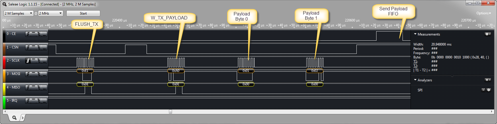
W_TX_PAYLOAD command with Flush
Interrupts
As pointed out above, I’m not setting the interrupt mask bits in the CONFIG register. In my application, I route the interrupts to the following handler, both for the sender and receiver:
static volatile bool isrFlag; /* flag set by ISR */

void APP_OnInterrupt(void) {
  CE_ClrVal(); /* stop sending/listening */
  isrFlag = TRUE;
}
I’m only setting a flag in the interrupt routine and pulling CE low to stop listening (if I’m listening). That function is called from Events.c:
/*
** ===================================================================
**     Event       :  IRQ_OnInterrupt (module Events)
**
**     Component   :  IRQ [ExtInt]
**     Description :
**         This event is called when an active signal edge/level has
**         occurred.
**     Parameters  : None
**     Returns     : Nothing
** ===================================================================
*/
void IRQ_OnInterrupt(void)
{
  APP_OnInterrupt();
}
Inside my sender main loop, I’m checking that interrupt flag and reset the STATUS flags as needed:
if (isrFlag) { /* check if we have received an interrupt */
  isrFlag = FALSE; /* reset interrupt flag */
  status = RF_GetStatus();
  if (status&RF24_STATUS_RX_DR) { /* data received interrupt */
    RF_ResetStatusIRQ(RF24_STATUS_RX_DR); /* clear bit */
  }
  if (status&RF24_STATUS_TX_DS) { /* data sent interrupt */
    cntr = 0; /* reset timeout counter */
    LEDR_Off(); /* indicate data has been sent */
    RF_ResetStatusIRQ(RF24_STATUS_TX_DS); /* clear bit */
  }
  if (status&RF24_STATUS_MAX_RT) { /* retry timeout interrupt */
    RF_ResetStatusIRQ(RF24_STATUS_MAX_RT); /* clear bit */
  }
}
This then looks like this:

Interrupt after data has been sent
Resetting the interrupt bit is needed to get the IRQ line back to HIGH. The zoom below shows that sequence in more details: It queries the status (0xFF instruction) which returns 0x1E (max retry reached, all FIFOs empty). Then it uses 0×27 command to reset the 0×10 bit.

Resetting Interrupt Flag
If data has been sent and acknowledge received, the 0×20 bit is set:

Interrupt with successful data sent
Receiver
Things are very similar on the receiver side: I check if an interrupt occured, then checking the flags. If the STATUS_RX_DR bit is set, it reads the data with RxPayload():
if (isrFlag) { /* interrupt? */
  isrFlag = FALSE; /* reset interrupt flag */
  cntr = 0; /* reset counter */
  LEDB_Off();
  LEDG_Neg(); /* blink green LED to indicate good communication */
  status = RF_GetStatus();
  if (status&RF24_STATUS_RX_DR) { /* data received interrupt */
    RF_RxPayload(payload, sizeof(payload)); /* will reset RX_DR bit */
    RF_ResetStatusIRQ(RF24_STATUS_RX_DR|RF24_STATUS_TX_DS|RF24_STATUS_MAX_RT); /* make sure we reset all flags. Need to have the pipe number too */
  }
  if (status&RF24_STATUS_TX_DS) { /* data sent interrupt */
    RF_ResetStatusIRQ(RF24_STATUS_TX_DS); /* clear bit */
  }
  if (status&RF24_STATUS_MAX_RT) { /* retry timeout interrupt */
    RF_ResetStatusIRQ(RF24_STATUS_MAX_RT); /* clear bit */
  }
} else {
  cntr++;
  if (cntr>500) { /* blink every 500 ms if not receiving data */
    cntr = 0; /* reset counter */
    LEDG_Off();
    LEDB_Neg(); /* blink blue to indicate no communication */
  }
  WAIT1_Waitms(1); /* burning some cycles here */
}
The receiver routine is similar to the sender one:
/*!
 * \brief Receive the Rx payload from the FIFO and stores it in a buffer.
 * \param payload Pointer to the payload buffer
 * \param payloadSize Size of the payload buffer
 */
void RF_RxPayload(uint8_t *payload, uint8_t payloadSize) {
  RF_CE_LOW(); /* need to disable rx mode during reading RX data */
  RF_ReadRegisterData(RF24_R_RX_PAYLOAD, payload, payloadSize); /* rx payload */
  RF_CE_HIGH(); /* re-enable rx mode */
}
It is using a method which reads the multiple payload bytes:
/*!
* \brief Read multiple bytes from the bus.
* \param reg Register address
* \param buf Buffer where to write the data
* \param bufSize Buffer size in bytes
*/
void RF_ReadRegisterData(uint8_t reg, uint8_t *buf, uint8_t bufSize) {
  RF_CSN_LOW();
  (void)SPI_WriteRead(RF24_R_REGISTER|reg);
  SPI_WriteReadBuffer(buf, buf, bufSize);
  RF_CSN_HIGH();
  RF_WAIT_US(10);
}
That’s it .
With this I’m able to send and receive data.
Source Code
The source code of this application is available on GitHub here.
Summary
This tutorial does not cover all the powerful aspects of the nRF24L01+, but should get you up and running quickly. I plan to add more functionality in the future and to create a dedicated Processor Expert component for this RF chip. Until then, I hope this tutorial is useful for you.
Happy Communicating